Call us now :07971406055

 Send Inquiry
Design and Development Electronics PCB for Job work
Price 1050.0 INR/ Unit
MOQ : 1 Unit
Design and Development Electronics PCB for Job work Specification
- Product Type
- PCB Design
- Material
- FR4 Epoxy, Copper Clad
- Power
- Custom/Project Specific
- Frequency (MHz)
- DC to 300 MHz (Design Capability)
- Working Temperature
- -40C to +85C
- Noise Level
- Passive (No Acoustic Noise)
- Dimension (L*W*H)
- Custom as per Design
- Weight
- Depends on Board Size & Layers
- Color
- Green, Blue, Black, Red, Custom Solder Mask
- Silkscreen Color
- White, Yellow
- Copper Thickness
- 0.5oz - 3oz
- Testing
- 100% Electrical Testing
- Software Support
- Altium Designer, Eagle, OrCAD, KiCAD, Protel
- Max Board Size
- Up to 600mm x 500mm
- Number of Layers
- 1-16 Layers
- Minimum Track Width/Spacing
- 0.1mm / 0.1mm
- Production Lead Time
- 2-3 Weeks
- Applications
- Consumer Electronics, Automotive, Industrial Controls, Medical Devices
- Surface Finish
- HASL, ENIG, OSP, Immersion Silver
- Prototype Lead Time
- 5-7 Days
Design and Development Electronics PCB for Job work Trade Information
- Minimum Order Quantity
- 1 Unit
- FOB Port
- Delhi
- Payment Terms
- Cash Advance (CA), Cash in Advance (CID), Cheque
- Delivery Time
- 7 Days
- Sample Policy
- Contact us for information regarding our sample policy
- Packaging Details
- BOX
- Main Domestic Market
- North India
- Certifications
- ISO 9001:2015
About Design and Development Electronics PCB for Job work
We are a well-known manufacturer and supplier of Electronic PCB Card designing & Development for Job work. These are madeby using optimum quality raw material under the guidance of our senior experts. These are also checked on various quality check parameters by our quality experts to maintain its good quality and to make sure the delivery of the best quality product. These are mainly used in industries. It is also available to our customers on budget-friendly price.These Electronic PCB Card are made by using iron material which makes it corrosion resistant. Any further information, you freely connect with us.Versatile PCB Capabilities
From single-layer prototypes to intricate 16-layer PCBs, our services are engineered for adaptability. We accommodate custom board sizes up to 600mm x 500mm, supporting projects in various sectors such as automotive, medical, and industrial control. Our solutions include a diverse palette of solder mask and silkscreen colors, optimizing both performance and appearance.
Precision Engineering and Quality Assurance
We maintain strict quality standards with minimum track width and spacing of 0.1mm, and complete 100% electrical testing for every board. Advanced surface finish options and material choices like FR4 epoxy ensure both longevity and reliability, even under demanding environmental conditions ranging from -40C to +85C.
Streamlined Process and Software Support
Our streamlined workflow, from design to delivery, leverages industry-leading software including Altium Designer, Eagle, OrCAD, KiCAD, and Protel. Customers benefit from fast turnaround with prototypes in just 57 days and production boards in 23 weeks, ensuring swift product development cycles.
FAQs of PCB Design and Development:
Q: How do I select the appropriate number of layers and copper thickness for my PCB project?
A: The choice depends on your circuit complexity and current requirements. Multi-layer PCBs (up to 16 layers) are suited for compact, high-performance designs, while copper thickness (0.5oz 3oz) should correspond to your applications power handling needs. Our team can assist you in determining the right configuration based on your specifications.Q: What surface finish and silkscreen options are available for these PCBs?
A: We offer multiple surface finishes including HASL, ENIG, OSP, and Immersion Silver, enhancing solderability and longevity. Silkscreen colors available include white, yellow, and custom options to meet identification and aesthetic preferences for your product.Q: When can I expect delivery for prototypes and bulk production orders?
A: Prototype boards are typically ready in 57 days after design approval, while production orders require 23 weeks. Timelines may vary depending on board complexity and order volume, but we strive for prompt and reliable delivery.Q: Where can these PCBs be used and what industries do you serve?
A: Our PCBs are suitable for consumer electronics, automotive, industrial control, and medical devices. We serve manufacturers, engineers, and OEMs as a distributor, supplier, manufacturer, and trader across India.Q: What is the process of PCB design, fabrication, and testing with your company?
A: Clients submit their PCB designs in supported software formats (Altium Designer, Eagle, OrCAD, KiCAD, or Protel). After review and approval, boards are fabricated with 100% electrical testing conducted. We prioritize communication and transparency throughout prototyping and production stages.Q: What are the benefits of using custom PCBs with controlled track width/spacing and multiple finish options?
A: Custom PCBs with fine track widths (0.1mm) allow for higher circuit density and reliability in compact devices. Multiple finishes ensure better soldering performance, while different silkscreen choices aid in component identification and branding, leading to robust products tailored to your requirements.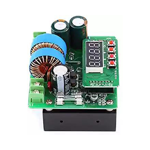
Tell us about your requirement

Price:
Quantity
Select Unit
- 50
- 100
- 200
- 250
- 500
- 1000+
Additional detail
Mobile number
Email

"We are dealing in North India Only."
Our Products

Plot No. 1, Brahmpuri Phase-1, Ranhola, Nangloi, Near Petrol Pump, New Delhi - 110041, India

Mr Mohd Jawed Nehal
(Director)
Mobile :07971406055
 Send Inquiry
 Send SMS
Developed and Managed by Infocom Network Private Limited.
